Research
Topics
Electromagnetic Compatible Design of Electrical and Electronic Devices and Systems
The purpose of this project is to improve an environment to design complicated electronic systems taking into account the reduction of electromagnetic interference (EMI) at the initial design stage. For example, we have developed a physics-based model for clarifying the mode conversion mechanism between normal mode and common mode at the interface where two transmission lines with different imbalance factors. The concept of imbalance matching based on the model helps effectively consider countermeasures against common-mode noise. In addition, we are currently improving the measurement technique for model validation, building up a new theory for high-speed digital circuit design, and so on.
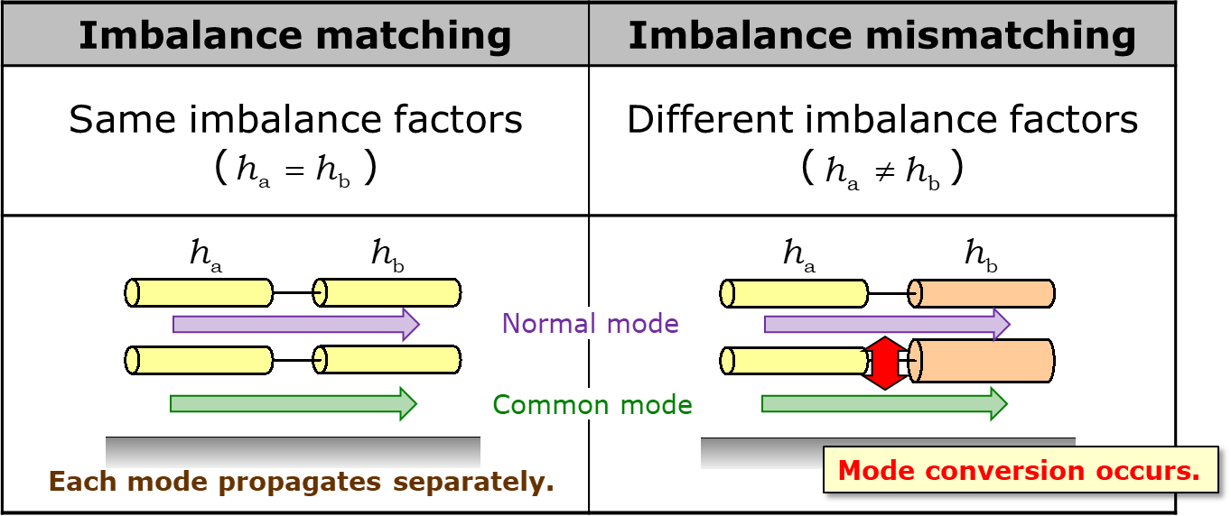
Imbalance mismatch causes mode conversion.
Control of Electromagnetic Wave Propagation by Periodic Structure
The power distribution/delivery network (PDN) in the printed circuit board (PCB) locally distributes power to system components. PDN consists of wires, traces, vias, and components such as capacitors. The requirements of PDN are to keep supply voltage constant within a narrow tolerance band and prevent high-frequency noise from propagating through PDN. We propose several new technologies for RF noise suppression. One of them is the RL snubber that consists of a parallel RL circuit inserted in series to resonant loop and minimizes the Q factor of the resonant loop by optimizing the values of R and L. The next example is an electromagnetic bandgap (EBG) structure with lossy material. The EBG structure works as a band elimination filter, and its stopband is formed with high attenuation by periodic structure.
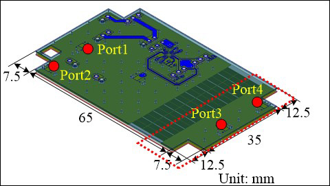
Test vehicle where IDE-EBG is installed.
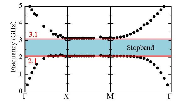
Dispersion diagram of IDE-EBG.
Measurement, Modeling, and Simulation of EMC Characteristics of Semiconductor Devices
In order to predict unintended emissions from electrical and electronic circuits and systems, it is inevitable to model the characteristics of semiconductor devices as a noise source. Our modeling target is not only digital circuits but also power conversion circuits. It is important to improve the measurement and simulation techniques for model validation.
Modeling and Simulation of Side-Channel Attacks to Cryptographic Devices
A side-channel attack (SCA) is a cryptanalytic attack that uses cryptographic devices' physical behaviors such as electromagnetic emanation and voltage fluctuation while processing cryptographic operations. Designing cryptographic devices secure against SCA is becoming more important as the devices are getting implemented on a wider variety of electronic products. Modeling and simulation of SCA will give useful knowledge such as how information leaks from the cryptographic devices and/or what parts of the device leak information. With the knowledge, designing cryptographic devices secure against SCA could become easier. The modeling and simulation of SCA will also give a prediction in vulnerabilities of their products to SCA. We developed an equivalent circuit modeling methodology of cryptographic devices that allows designers to simulate SCA vulnerability. Model parameters are identified both from the design information of cryptographic devices and measurements after the fabrication.
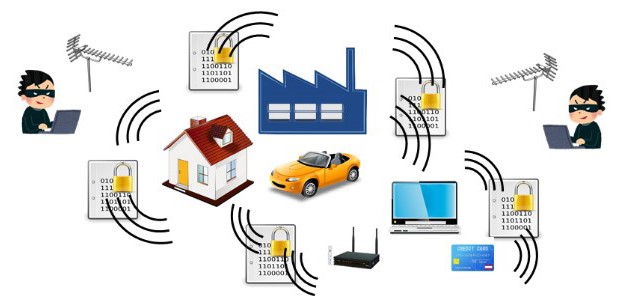
Side-channel attack abusing electromagnetic leakage.
Equipment and Simulators
Measurement or Evaluation Equipment
- Oscilloscopes
- Vector network analyzers
- Spectrum analyzers
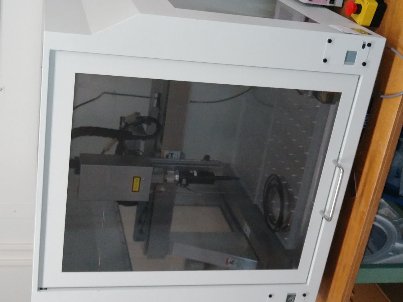
- 4EM500 Near-field Scanner System (NEC Engineering)
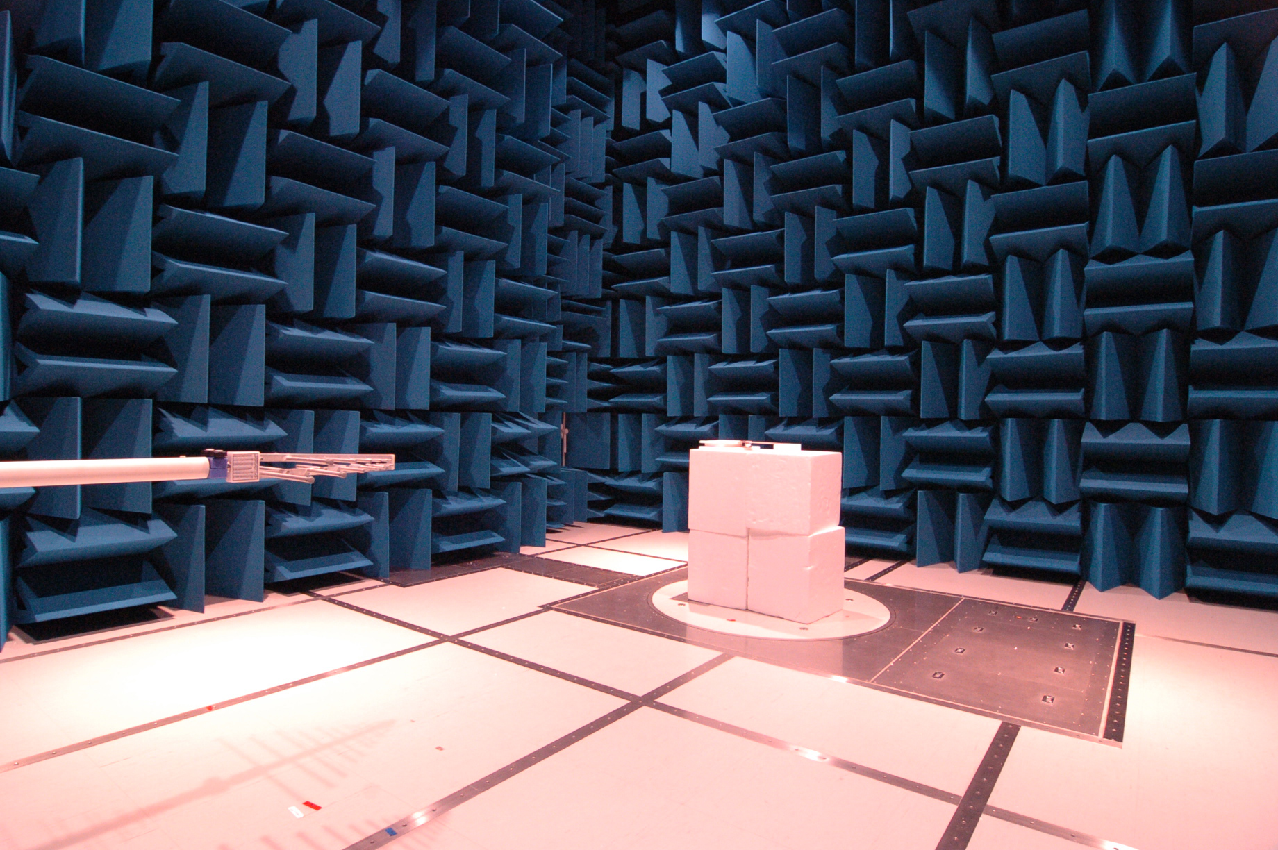
- ALC-3N9053 Semi-anechoic Chamber (3m法 | Tokin)
Simulators
- Ansys HFSS
- Keysight ADS
- Cadence AWR Microwave Office
